|
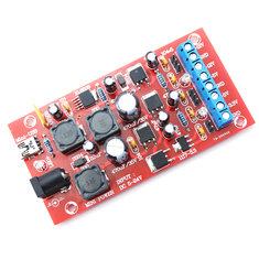
With this € 6.09 priced kit, you can convert one supply voltage into stabilized supply voltages of +3.3 V, +5 V, -5 V, +12 V and -12 V. You can load each output individually up to 300 mA. We built and tested one kit. |
Introduction to the SKU332561 kit
Who makes it and what is its name?
This kit is probably made by Hiland, but is not so easy to find on Google. We identify it in this article by means of the unique SKU code, the 'Stock Keeping Unit' code. You can use this code to find the kit via Google if you want to order it somewhere. That code is SKU332561.
Where can you use this PCB?
If you build a circuit that only needs one supply voltage, there is no problem. You supply this circuit from an adjustable power supply or from an AC adapter that provides the right voltage. However, there are circuits that require two or sometimes four different supply voltages. Without this SKU332561 PCB, you would have a big problem: where do all these voltages come from? With this SKU332561 your problem is solved. This PCB derives all standard supply voltages from one input voltage:
+3.3 V
+5.0 V
-5.0 V
+12.0 V
-12.0 V
The components of the kit
The delivered components look excellent. However, the six ICs are supplied in SMD version, the same is true for two diodes and three coils. This requires experience with soldering small components.
As usual with Chinese building kits, this universal power supply board is supplied without manual, you must use the component print on the PCB to solder the parts in the right places.
 |
| The components supplied and the PCB are of excellent quality. (© 2019 Jos Verstraten) |
The complete schematic diagram of this multi-output power supply is shown in the figure below. On the left side the input voltage is applied. The UF300 is a self-restoring 3 A fuse. The presence of input voltage and the proper functioning of the fuse are checked by the LED HL1. You can divide the diagram into two parts. On the left is a buck converter around an XL6008, which converts the input voltage into stable +16 V and -16 V output voltages. These output voltages are set by the ratio between the resistors R2 and R3. Thanks to the built-in MOSFET with an extremely low resistance of 120 mΩ, the IC can handle up to 3 A current. This results in an efficiency of more than 90 %, so hardly any power is lost in the chip. The oscillator operates at 400 kHz, you can work with very small coils and capacitors to smooth the output voltages. The positive voltage of 16 V is available over the capacitor C4, the negative voltage of -16 V over the capacitor C6.
 |
| The complete schematic diagram of this quintuple power supply. (© Banggood) |
With the linear section, however, something strange is happening. In the negative section, the -16 V is first converted to -12 V via a 7912 and this is reduced with a 7905 to -5 V, as it should be according to theory. In this way, the large residual power that arises when you load the -5 V output is divided between the 7912 and the 7905. However, the two positive controllers 7805 and 7812 are parallel and both retrieve their input voltage from the +16 V. So if you load the +5 V with the specified maximum output current of 300 mA, the 7805 consumes no less than 3.3 W. However, the 7805 is cooled in the same way as the other stabilizers, namely with a heatsink of only 10 mm x 10 mm x 5 mm. We will come back to this later in the test.
The specifications of the SKU332561
- Input voltage: 5.0 Vdc ~ 24.0 Vdc
- Output voltages: +3.3 Vdc, +5.0 Vdc, +12.0 Vdc, -5.0 Vdc, -12.0 Vdc
- Output current: 300 mA per output, one output loaded
- Output current: 200 mA per output, multiple outputs loaded
- Dimensions: 10.0 cm x 5.0 cm
The construction of the PCB
First the SMDs .......
On the forum of one of the suppliers it is recommended to first coat the six copper squares on the copper side of the PCB with tin. It's a matter of creating a volume in which the heat can be stored, probably. Afterwards comes an annoying job: soldering the eleven SMD components. Don't start without a miniature soldering iron with an extremely fine tip! Also a pair of tweezers and a magnifying glass are indispensable for this piece of work.
Not all readers will have experience working with SMD's. The procedure for soldering such parts is as follows. Tin one of the copper surfaces on the PCB with a thin layer of tin. Place the SMD at its position and place the tip of the soldering iron at the contact that rests on the tinned surface. If this one contact is fixed, you can solder the remaining contact(s) very carefully and with very little tin. You have to position the part on the PCB in such a way that there is room to solder the very small cooling clip on the copper surface on the PCB.
When soldering the two diodes, pay attention to the white stripe on the diode, which corresponds to the thick white area on the component print.
 |
| The location of the eleven SMDs on the PCB. (© 2019 Jos Verstraten) |
Afterwards you can solder the other parts. For the LEDs you must remember that the long wire corresponds to the anode. With the electrolytics the negative connection is at the shaded part of the PCB. After completion of the soldering work you must glue the supplied miniature heatsinks to the six ICs. The result of the assembly is shown in the picture below.
 |
| The fully assembled PCB. (© 2019 Jos Verstraten) |
Testing the SKU332561
Test 1: the operation of the XL6008
The operation of this multi-output power supply is of course determined by the circuit around the XL6008. How good is this buck-converter capable of deriving two stable voltages of +16.5 V and -16.5 V from an input voltage that may vary between 5.0 V and 24.0 V? This part of the circuit works excellently. We loaded the five outputs with 1 kΩ resistors and we varied the input voltage between 24.0 V and 3.0 V. Up to 4.0 V, the two output voltages of the buck-inverter remained constant at +16.28 V and -16.34 V up to 10 mV. At an input voltage of 3.0 V, the output voltages dropped to +14.81 V and -15.13 V.

It is very strange, however, that at the output voltage a large ripple with a peak-to-peak value of 5 V and a frequency of 117 Hz can be measured, see the oscillogram below. This phenomenon cannot be explained by the XL6008's operation.
 |
| The big ripple at the output of the buck-converter XL6008. (© 2019 Jos Verstraten) |
We have performed these and the following tests with input voltages of 5.0 V and 12.0 V, because in practice you will usually power this PCB from a 5 V USB power supply or a 12 V AC adapter. The results of this test are shown in the table below. With a 12 V power supply, the PCB behaves well up to 400 mA load. With a 5 V power supply, the +12.0 V output at 300 mA collapses completely.
 |
| Testing the +12.0 V output. (© 2019 Jos Verstraten) |
Of course we repeated these measurements for the -12.0 V output, with the results below. These results are much worse. At a load current of only 200 mA there is an enormous ripple at the output voltage, see the oscillogram below. This ripple disappears when the input voltage is set a little lower.
 |
| Testing the -12.0 V output. (© 2019 Jos Verstraten) |
 |
| The ripple on the -12.0 V output at a load current of 200 mA and an input voltage of 12.0 V. (© 2019 Jos Verstraten) |
The same measurements, with the measuring equipment now at the +5.0 V output, with the results below.
 |
| Testing the +5.0 V output. (© 2019 Jos Verstraten) |
This output behaves well up to 300 mA. At 400 mA, however, a huge ripple is created on the output at 12.0 V input voltage.
 |
| Testing the -5.0 V output. (© 2019 Jos Verstraten) |
This voltage remains good under all load conditions, see table below. Also the ripple at the output is minimal.
 |
| Testing the +3.3 V output. (© 2019 Jos Verstraten) |
It turns out that the supplied miniature heatsinks are too small for the power supply to meet the specifications under all circumstances. With a 12.0 V supply, the output voltages at a current of 250 mA are interrupted after a few minutes because the chips become too hot and the built-in temperature protections are activated. This applies to voltages of +5.0 V, -5.0 V and +3.3 V.
General conclusion
This quintuple power supply PCB is ideal if you do not load the outputs with more than 200 mA. The maximum load current of 300 mA per output specified by the manufacturer is not realistic because the heatsinks on the chips are too small.
We have not been able to check how this power supply behaves when you simultaneously load all five outputs to the maximum, due to the lack of sufficient high-power resistors and with only one adjustable electronic load available. However, we suspect from our tests that this PCB is absolutely not capable of meeting the specifications if all outputs are loaded to the maximum.

Linear Regulators Multiple Output Power Kit