|
With this small PCB you can convert a DC voltage of at a least 3.0 V to a DC voltage up to 40.0 V, according to the specifications. The maximum output current varies from 2 A at 35 V to 1 A at 5 V on the output. |
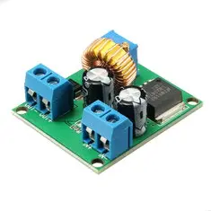
Introduction to the HW-637
The PCB of the HW-637
The HW-637 is for sale in China from € 1.02 per piece. Search for 'HW-637' or for 'DC-DC 3 V-35 V to 4 V-40 V Step Up Power Module Boost Converter'. The printed circuit board is delivered ready to use and measures 37 mm by 32 mm by 15 mm. On one side there are two screw terminals for connecting the input voltage and the output voltage. The negative poles of both voltages are galvanically connected and represent the common ground of the circuit. On the other side of the PCB you notice a miniature multiturn potentiometer, with which you can set the output voltage to the desired value. One IC, an LM2587S-ADJ in 5-pin DDPAK/TO-263 housing, is soldered to the ground plane of the PCB. This surface is in contact with the ground plane on the backside of the PCB through a number of plated through holes.
Between the two screw terminals is a small red LED that is connected to the output voltage via a series resistor.
 |
| The two sides of the PCB of the HW-637. (© 2020 Jos Verstraten) |
This chip is officially a Step Up Wide VIN Flyback Regulator. The internal block diagram is drawn in the figure below. The electronic switch is not a MOSFET, as can be expected, but a bipolar NPN transistor with a maximum collector current of 5 A. The internal oscillator operates at about 100 kHz. The circuit is equipped with a soft-start function, which causes the output voltage to rise with a certain delay and prevents large start-up currents. An internal protection reduces the dissipated power by decrease the output voltage when the chip gets warmer than +125°C. The output stabilization is a bit disappointing. According to the specifications, the output voltage drops by up to 100 mV at an output voltage of 12.0 V and a load of 1.75 A. Also the switching ripple on the output is quite large: the data sheet mentions a value of at least 100 mVpeak-to-peak at 1 A. The efficiency of the chip is around 70 %.
 |
| The internal block diagram of the LM2587S-ADJ. (© 2019 Texas Instruments) |
Based on the example circuit diagrams in the data-sheet and the traces on the PCB, it is not difficult to reconstruct the schematic of the HW-637. As can be seen from the figure below, the designers follow the guidelines of the chip manufacturer. What is noticeable, however, is that in some cases other component values are used than those prescribed by the manufacturer.
The functioning of the circuit can be briefly described as follows. If the NPN output transistor in the chip is in the saturated state, current flows through coil L1. This current will rise to its maximum value, determined by the input voltage and the inductance of the coil. Electrical energy is stored in the coil. When the power transistor is in the cut-off state, the energy stored in the coil will cause the voltage on pin 4 to be many times higher than the supply voltage. The schottky diode D1 conducts and transfers the voltage over the coil to the output capacitor C4. By varying the duty-cycle of the output transistor, you can set the output voltage to the desired value.
 |
| The schematic of the HW-637. (© 2020 Jos Verstraten) |
The HW-637 step up boost converter tested
Output voltage range
We powered the circuit with 5.0 V and rotated the adjustment potentiometer over the full range. The end values of the output voltage at zero load:
- Minimum value: 4.80 V
- Maximum value: 30.95 V
Minimum input voltage for 30.0 V output voltage
The output voltage was adjusted to 30.0 V at 5.0 V at the input. At zero load, we could reduce the input voltage to 2.91 V before the output voltage decreased.
No load power consumption of the circuit
An important factor is the no load power consumption. This is certainly important with battery operated devices, where these inverters are often used. The PCB was powered with 5.0 V and the output voltage was set to the usual supply voltages. The current consumption from the input voltage was measured. In the table below, these measurements are summarized and also the no load power consumption is calculated.
 |
| The no load power consumption of the HW-637. (© 2020 Jos Verstraten) |
At 5.0 V at the input, the output voltage was adjusted to 30.0 V. Afterwards the input voltage was varied between 3.0 V and 24.0 V and the input stabilization of the circuit was measured.
 |
| The input stabilization of the HW-637. (© 2020 Jos Verstraten) |
If you set the output voltage of the HW-637 to 30.0 V and load the PCB with 1 A current, the inverter delivers 30 W of power. You have to offer that power at the input as well. If you set the input voltage to 5.0 V, this power supply will have to supply at least 6 A! Of course, this circuit also has an efficiency of less than 100 %, so count on more input current than the calculation example shows.
Our lab power supply delivers a maximum current of 3 A. That is why we have not been able to test the HW-637 to its maximum current under all circumstances. However, the three examples of the tested output stabilization will still give you a good impression of the capacity of this small PCB.
Output stabilization from 5.0 V to 12.0 V
In the table below we have tested the output stabilization at 5.0 V at the input and 12.0 V at the output. We loaded the PCB with a digitally adjustable current sink. In the table you see not only the deviation of the output voltage, 40 mV over 800 mA, but also the input and output power. By a simple division, you can calculate the efficiency of the circuit from these two data.
 |
| Output stabilization from 5.0 V to 12.0 V. (© 2020 Jos Verstraten) |
The same test with an output voltage of 30.0 V. In this test, our input power supply already reached its current limitation of 3.0 A at an output load of 300 mA.
 |
| Output stabilization from 5.0 V to 30.0 V. (© 2020 Jos Verstraten) |
Finally from 5.0 V to 24.0 V. Now our 3.0 A power supply can keep it up to an output current of 400 mA. As you can see from the table, the PCB behaves nicely. Over 400 mA, the output voltage only drops by 50 mV.
 |
| Output stabilization from 5.0 V to 24.0 V. (© 2020 Jos Verstraten) |
At an input voltage of 5.0 V, the output voltage was set to 12.0 V. At four load currents, the maximum temperature was measured on the surface of the LM2587S-ADJ. A type-K thermocouple was used, which was in good thermal contact with the surface by means of cooling paste. The data below are of course the stabilised temperatures, it sometimes takes more than ten minutes for the chip to reach this final temperature:
- 500 mA: +52.0 °C
- 600 mA: +65.6 °C
- 700 mA: +75.4 °C
- 800 mA: +88.9 °C
The efficiency of the circuit
The efficiency is nothing more than the power provided by the circuit divided by the input power to the circuit. The higher the efficiency, the less power is lost in the circuit and the longer the batteries last. The previous three tables show that the measured efficiency varies between 63 % and 77 %, values that are in accordance with the specifications.

The noise and ripple behaviour of the HW-637
The used switching principle means that there is always some residue of the switching frequency on the output. However: the less, the better!
At an input voltage of 5.0 V, the output voltage is set to 24.0 V. The circuit was tested with 400 mA. The noise and ripple on the output voltage are measured directly on the terminals of the printed circuit board with the oscilloscope, see pictures below. With a peak-to-peak value of more than 400 mV, it is not possible to talk about a ripple-free output voltage. In the right picture, the period of the ripple was measured as 20.80 μs, from which a switching frequency of 48.0 kHz is calculated. This is strange, because this value is far beyond the value of 100 kHz specified in the data sheet. The measurements were repeated for other combinations of input and output voltages and loads, but each time a value around 50 kHz was measured.
 |
| Noise and ripple on the 24.0 V output at 5.0 V input and 400 mA load. (© 2020 Jos Verstraten) |
As a final test, the PCB was loaded with a rectangular current pulse with a value of 400 mA and a frequency of 1 kHz, at 24 V at the output and 5 V at the input. In the picture below you can see in the lower trace the base signal of the 2N3055 that we used as load and above the ripple on the output voltage of the HW-637. A ripple of almost 2.0 V on an output voltage of 24.0 V is of course quite a lot! To make the 1 kHz ripple clearly visible, the 'Average' mode of the oscilloscope was activated, so the non synchronized 50 kHz ripple of the internal switch was removed from the image.
 |
| The dynamic behaviour at 1 kHz, 5 Vin, 24 Vout and 400 mA pulse current load. (© 2020 Jos Verstraten) |
Our conclusion on the HW-637
If you need to design a circuit that is powered by batteries and needs a higher supply voltage than the batteries provide, you can use this HW-637 to generate this higher supply voltage without much difficulty. You can't make it any cheaper yourself! Because of the rather high ripple on the output, however, you will have to apply extra smoothing and perhaps even stabilization to the supply voltage of sensitive circuits.

HW-637 step up boost converter