|
A famous transistor amplifier, designed in 1969, is back on the market and offered as a cheap kit in China. We bought one, built it and performed some tests. |
What is the Linsley-Hood 1969 amplifier?
Who was Linsley-Hood?
John Laurence Linsley-Hood, born in 1925 and died in 2004, was an English electronics engineer best known for designing audio circuits. His circuits with transistors were at least as good as the well-known circuits with tubes that were common at the time. One of his most famous designs was the 'Simple Class A Amplifier' published in the April 1969 issue of Wireless World. It was a very simple transistor power amplifier that, a revolution in those days, did not work in class B or class AB, but in class A. We have retrieved the original article from the internet and saved it as a PDF file on our Google Drive account:
➡ Simple_Class_A_Amplifier.pdf
This amplifier was designed as a transistor alternative for the well-known Williamson amplifier from 1947. This circuit was a class A amplifier with triodes and was for decades the standard DIY amplifier.
The measurements published in the article revealed that the Linsley-Hood amplifier had a total harmonic distortion of only 0.05 % at 9 W output power and 1 kHz sine wave as test signal. That was an unprecedented low value for a transistor amplifier at that time. However, it should be noted that the transistors were selected to provide the largest possible and almost identical current gain.
What is a class A amplifier?
The figure below shows a simplified circuit diagram of the output stage of an analogue transistor audio amplifier. The connection between both power transistors T2 and T3 is set to half of the supply voltage +Ub. Almost all such power amplifiers operate in class B or in class AB. With this setting of the output stage, no (B) or at most a small (AB) quiescent current Iidle flows through the two power transistors. In the positive half period of the input signal (red), a large signal current Iplus flows through the upper power transistor T2, the DC-blocking capacitor C1 and the loudspeaker LS1. In the negative half period (blue) an equally large signal current Iminus flows through the loudspeaker, the capacitor C1 and T3.
The problem with this kind of setting arises with small values of the signal. Then either both transistors conduct or does not conduct, causing so-called 'crossover' distortions on the output signal.
A characteristic of these settings is that the quiescent current Iidle is much smaller than the signal currents Iplus and Iminus.
 |
| The output stage of an analogue transistor audio power amplifier. (© 2022 Jos Verstraten) |
When the output stage is set to class A, a very large quiescent current Iidle flows through both output transistors. The two power transistors have a small resistance between the collector and the emitter. At the positive half period of the input signal, the two power transistors are controlled in such a way that the resistance of T3 increases and that of T2 decreases. The result is that the voltage at the junction of the two transistors increases and an current Iplus flows through capacitor C1 to the loudspeaker. With the negative half period, this situation is reversed, and the voltage at the junction decreases. The charge stored in the capacitor causes an opposing current Iminus to flow through the lower transistor T3 and the loudspeaker.
A characteristic of the class A setting, therefore, is that both power transistors conduct continuously and a very large quiescent current flows through these components. When the output stage is driven by a signal, this current will be modulated by the signal, but the average value of this alternating current will remain almost equal to the quiescent current flowing through the output stages.
The advantage of this setting is that the cross-over distortion so typical of a class B or class AB setting is absent. The disadvantage is that such an amplifier has a very low efficiency. You have to push a lot of supply power into the circuit to get a little loudspeaker power out of it. Of course, this has everything to do with the large value of the quiescent current, which also flows when the amplifier processes whisper-soft signals.
The Linsley-Hood 1969 DIY kit
Suppliers and prices
This amplifier is offered as a kit by almost all Chinese Internet companies. You can google terms like 'TTC5200 KIT', '1969 CLASS A', 'HOOD 1969', '1969 NPN'. You will notice that there are several versions in circulation that differ slightly from each other. In the picture below, we have collected a few of the available sets. Prices range from € 14.09 for a mono version over € 25.79 for the cheapest stereo version to over € 55.00 for exactly the same product. Some packages are delivered without the heatsink, others with the extra parts for the power supply. So pay attention to what is in the package! We ordered a package with heatsink but without power supply for € 25.78 including shipping from the 'Hi IC Store' via AliExpress, see the red arrow.
 |
| Several examples of this amplifier DIY kit. (© 2022 Jos Verstraten) |
The delivered components
As usual, the components are delivered sloppily packaged in a plastic bag. The quality of the supplied components is excellent. In the original design, Motorola MJ480 transistors are used in the output stage. In the package that we received, these have been replaced by four TTC5200 from Toshiba. In some deals it is mentioned that these power transistors are 'selected', without further explanation of what is meant by this. In the context of this design, this can only refer to the current gain, which must have approximately the same value for all four transistors. We have of course measured this with the following result:
- TTC5200 #1: HFE = 127
- TTC5200 #2: HFE = 127
- TTC5200 #3: HFE = 113
- TTC5200 #4: HFE = 115
The value specified by the manufacturer for the current amplification is between 80 and 160. So it seems that the transistors have indeed been selected, because otherwise the spread on this parameter would have been larger.
The heatsink measures 120 mm by 55 mm by 50 mm and is provided with six tapped holes. Four of these are obviously intended for mounting the transistors, and in the long side there are two holes for attaching the heatsink to the chassis of an enclosure. The four trimmer potentiometers are made by Benteng and are exact copies of the well-known Multiturn Trimpot's by Bourns.
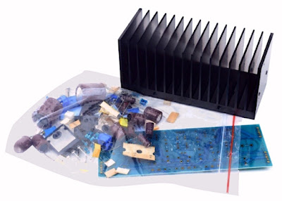 |
| The rather sloppy way in which the parts are delivered. (© 2022 Jos Verstraten) |
The technical specifications of the amplifier
According to the supplier, this amplifier has the following specifications:
- Supply voltage: 12 Vdc ~ 35 Vdc
- Quiescent current: 0.3 A ~ 1.5 A per amplifier (recommended 0.7 A @ 25 V)
- Output power: 10 W ~ 15 W
- Speaker impedance: 4 Ω ~ 16 Ω
- Dimensions: 130 mm x 50 mm x 85 mm
- Weight: 390 g
About distortion nothing is mentioned.

Missing building instruction
Our package did not contain a building instruction. It is true that the PCB has a component silkscreen, so that soldering the components on this board is not a problem. But then you don't know, for example, what to do with the four trimmer potentiometers. The lack of a sheet of paper that at least describes the schematic of the amplifier and the adjustment procedure is, in our opinion, absolutely unacceptable for any kit. This has to be improved!
The schematic of the amplifier
Fortunately, after some searching, the schematic can be found on the internet. We have drawn it neatly with sPlan from Abacom, with the below result. If you have taken the trouble to download the original article and look at figure 3, you will see that the circuit is identical to the original by Linsley-Hood, down to the smallest detail. Even the resistor values are identical! Only different types of transistors are used and it is remarkable that some resistors have a lower power than stated in the original diagram.
Capacitor C7 is only present once, the same goes for the LED and series resistor R11.
With the trimmer potentiometer R1 you can adjust the voltage between the two power transistors to half the supply voltage. R8 controls the value of the quiescent current through the output stage. Capacitor C4 is the so-called 'bootstrap' capacitor that ensures that transistor T3 still receives sufficient driving current at the base at positive peaks of the output signal.
The resistors R6 and R7 are very important, because they provide the only feedback present in the amplifier. The ratio between these two resistors not only determines the voltage gain of the circuit, but also the current stabilisation of the whole. This works as follows. If one of the power transistors is conducting more or less than intended, the voltage at the junction will deviate from ½Ub. This deviation will influence the conductance of transistor T1 via resistor R6. The voltage across resistor R3 varies and this in turn causes a deviation in the conductance of T2. The voltage across R9 will then also vary, resulting in the conductance of the transistor T4 being adjusted to compensate for the original imbalance.
The printed circuit board for the amplifier
This is double-sided and there is nothing to complain about. On one side, some tracks do not have a full solder mask. The intention is undoubtedly to make these tracks 'thicker' by applying a layer of solder. However, not all tracks of the output stage are equipped with this, so the usefulness of this treatment is doubtful.
- Speaker impedance: 4 Ω ~ 16 Ω
- Dimensions: 130 mm x 50 mm x 85 mm
- Weight: 390 g
About distortion nothing is mentioned.

Missing building instruction
Our package did not contain a building instruction. It is true that the PCB has a component silkscreen, so that soldering the components on this board is not a problem. But then you don't know, for example, what to do with the four trimmer potentiometers. The lack of a sheet of paper that at least describes the schematic of the amplifier and the adjustment procedure is, in our opinion, absolutely unacceptable for any kit. This has to be improved!
The schematic of the amplifier
Fortunately, after some searching, the schematic can be found on the internet. We have drawn it neatly with sPlan from Abacom, with the below result. If you have taken the trouble to download the original article and look at figure 3, you will see that the circuit is identical to the original by Linsley-Hood, down to the smallest detail. Even the resistor values are identical! Only different types of transistors are used and it is remarkable that some resistors have a lower power than stated in the original diagram.
Capacitor C7 is only present once, the same goes for the LED and series resistor R11.
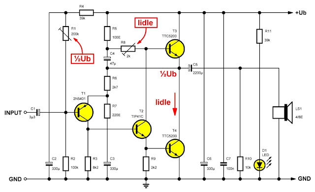 |
| The schematic of the Linsley-Hood 1969 amplifier. (© 2022 Jos Verstraten) |
With the trimmer potentiometer R1 you can adjust the voltage between the two power transistors to half the supply voltage. R8 controls the value of the quiescent current through the output stage. Capacitor C4 is the so-called 'bootstrap' capacitor that ensures that transistor T3 still receives sufficient driving current at the base at positive peaks of the output signal.
The resistors R6 and R7 are very important, because they provide the only feedback present in the amplifier. The ratio between these two resistors not only determines the voltage gain of the circuit, but also the current stabilisation of the whole. This works as follows. If one of the power transistors is conducting more or less than intended, the voltage at the junction will deviate from ½Ub. This deviation will influence the conductance of transistor T1 via resistor R6. The voltage across resistor R3 varies and this in turn causes a deviation in the conductance of T2. The voltage across R9 will then also vary, resulting in the conductance of the transistor T4 being adjusted to compensate for the original imbalance.
The printed circuit board for the amplifier
This is double-sided and there is nothing to complain about. On one side, some tracks do not have a full solder mask. The intention is undoubtedly to make these tracks 'thicker' by applying a layer of solder. However, not all tracks of the output stage are equipped with this, so the usefulness of this treatment is doubtful.
 |
| The two sides of the PCB. (© 2022 Jos Verstraten) |
Building the Linsley-Hood 1969 amplifier
The first step
There is no provision on the PCB to temporarily disconnect the two amplifiers from the power supply. Therefore, it is not possible to adjust the quiescent current through the output stages when the amplifier is built. An ammeter in the positive supply line always measures the sum current of both amplifiers. According to information we found on the internet, the quiescent current should be equal to 0.7 A per channel at 25 V supply voltage. Apparently, this current will flow through the output stage if you set the adjustment potentiometer R8 (2 kΩ) to a value of 930 Ω. From the picture below you can see between which terminals you have to measure this resistance value. Pay attention to the position of the adjustment screw, also when you solder these parts on the PCB!
 |
| Adjustment of the R8 potentiometer. (© 2022 Jos Verstraten) |
Assembling the PCB
Based on the picture below you can solder all components, except the four power transistors, in this order on the PCB:
- 17 resistors
- 1 LED, the cathode is the shortest connection wire
- 1 capacitor 100 nF
- 2 transistors 2N5401
- 3 printed circuit board terminal blocks
- 4 trimmer potentiometers, pay attention to the position!
- 12 elco's, mind the plus and the minus!
- 2 transistors TIP41C, pay attention to the position of the cooling tab!
A handy tip: do not cut the positive wires of the two electrolytic capacitors C5 (2,200 μF), but bend them to the sides of the PCB so they stick out. You can use these 'adjustment points' afterwards to adjust the ½Ub at the junction of the power transistors.
To connect the two input signals, a three-pole PCB header is supplied. Unfortunately, a cable connector for this is missing. Whether this is a convenient option in your case is up to you to decide. However, the three holes are very close together and the pads are much too small to fit solder tabs in the holes. So there is hardly any other option than to use the header.
 |
| The complete soldered circuit board. (© AliExpress) |
Mounting the four power transistors
The four power transistors are screwed to the sides of the heatsink using the four insulating plates provided. However, do not screw these parts tightly yet, but loosely enough so that they can still move. The idea is to push the 4 x 3 connection wires through the twelve holes of the PCB. You must do this in such a way that the PCB is about one centimeter above the heatsink and is of course completely parallel to this heatsink. When you have done that (you will have to bend the wires of the power transistors a bit and move the transistors to the left or to the right) you can solder the wires of the four transistors on the PCB. Then screw the semiconductors tightly onto the heatsink.
Remember that the cooling tab of the TTC5200 transistor is connected to the collector and that it is absolutely necessary that you insulate the four semiconductors on the heatsink.
In the picture below, between the two transistors, you can see the bent-up connecting wire of one of the capacitors C5 that you can use to adjust the trimmer potentiometer R1.
 |
| Mounting the power transistors. (© 2022 Jos Verstraten) |
The completely assembled amplifier
In the picture below you can see the end result of the building of this Linsley-Hood 1969 amplifier.
 |
| The completely assembled Linsley-Hood 1969 amplifier. (© AliExpress) |
Adjusting the amplifier
Connect the two inputs to ground and connect the PCB to an adjustable DC power supply that can deliver at least 2 A. Connect a DC multimeter between the ground and one of the wires sticking out left and right. Slowly increase the output voltage of the power supply to, for example, 12 V. Now turn the screw of the R1 trimmer potentiometer of the relevant channel until the meter reads 6 V. Then slowly increase the supply voltage to a maximum of 30 V and check during this process that the measured voltage remains approximately equal to half the supply voltage and that the current does not exceed 2 A. If necessary, adjust the trimmer potentiometer until the meter indicates half the supply voltage again.
Repeat for the second channel.
The wiring diagram
In the figure below, we have drawn the wiring diagram of this amplifier. Please note that both loudspeaker outputs are grounded with one pole. Also the negative pole of the power supply and the middle contact of the input connector are grounded. You must connect the shielding of the two input cables to this pin of the PCB header. To avoid ground loops, leave one of these shields open on the other side of the cable.
You should not feed the amplifier from a modern switched mode power supply, the chance that HF interference will penetrate the amplifier is very high. So you must use an old fashioned linear power supply, consisting of a 50/60 Hz transformer, a bridge rectifier and a large smoothing capacitor. The amplifier can be powered with a maximum DC voltage of 35 V. This means that you can use a transformer with an unloaded secondary winding of 24 V maximum. This transformer must be able to deliver 3.0 A.
 |
| Wiring diagram of the amplifier. (© 2022 Jos Verstraten) |
Testing the Linsley-Hood 1969 amplifier
The power supply
We powered the PCB with a well smoothed 30 Vdc voltage from an analogue power supply. To be able to deliver current peaks, the output voltage was buffered additionally with ten 1,000 μF electrolytic capacitors connected in parallel. The delivered current is 2.2 A which means that the quiescent current is apparently 1.1 A per amplifier. It is a pity that this cannot be checked and corrected quickly without intervening in the PCB!
The maximum power
We connected both outputs to a wirewound resistor of 8 Ω. The two inputs are connected in parallel to a 1 kHz sine wave voltage. If you increase this voltage, the output voltages of the amplifiers will clamp against ground and the power supply at a certain moment. That is called 'clipping of the output voltage'. The idea then is to reduce the input voltage a little and measure the output voltage. In our amplifier 8.8 Vrms was measured across the load resistors of 8 Ω. The power that is generated in a resistor is equal to:
P = U²/R
In this case, this gives a power output of 9.68 W. With 4 Ω load resistors, we measure a voltage before clipping of 6.4 Vrms, so an output power of 10.2 W.
The signal amplification
This is measured with an 8 Ω load. With a sine wave of 500 mVrms at the input, we measure a sine wave of 6.58 Vrms at the output. This corresponds to a voltage gain of 13.16 or 22.38 dB.
Noise and hum
We have short-circuited the three pins of the input connector and measured the signal at the outputs of the amplifiers. At the right channel we measured 2.7 mV noise and hum, at the left channel 3.1 mV.

The amplitude/frequency characteristic
We measured these at a load resistance of 8 Ω and a power of 5 W. As a reference, we naturally chose a sinusoidal signal with a frequency of 1 kHz. The results are impressive and are summarised in the graph below. The -1 dB frequencies are at 22 Hz and 181 kHz. Above 50 kHz there is a small boost with a peak of +0.5 dB at 64 kHz. At 10 Hz and at 311 kHz the gain is reduced by 3 dB. The -1 dB point can be decreased a little by choosing higher values for capacitors C1 and C5.
However, it must be noted that above 100 kHz, a clearly visible distortion occurs in the edges of the sine signal.
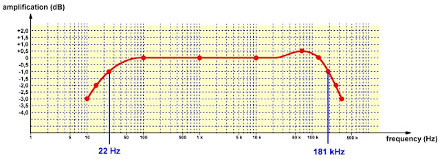 |
| The amplitude/frequency characteristic. (© 2022 Jos Verstraten) |
The reproduction of rectangular signals
In the figure below, we have connected square waves of 100 Hz, 1 kHz and 10 kHz to the Linsley-Hood 1969 amplifier. The peak to peak value of the signals is 15 V. The yellow traces give the output voltage of the right channel, the blue of the left channel. The measured large bandwidth translates into the good reproduction of a square wave with a frequency of 10 kHz.
 |
| The reproduction of rectangular signals. (© 2022 Jos Verstraten) |
A closer look at the 'ringing'
From the reproduction of the 10 kHz square wave, you can see that the amplifier is rather critical in its tendency to generate HF oscillations under certain input conditions, such as fast signal transitions. Such a phenomenon is called 'ringing'. These unwanted HF signals arise due to the presence of parasitic capacitances and inductances in the design of the amplifier. The very large bandwidth obviously contributes to the occurrence of this phenomenon. A small capacitor across the feedback resistor R6 would probably have suppressed this phenomenon. We have examined this ringing in detail, see the oscillogram below. It shows that this ringing has a frequency of approximately 280 kHz.
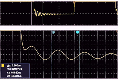 |
| Detail of the ringing. (© 2022 Jos Verstraten) |
The phase behaviour of the amplifier
A good amplifier must not introduce a phase shift between the input and output signal. It becomes even more disastrous if this phase shift is also frequency-dependent. We have investigated this at frequencies of 100 Hz, 1 kHz and 10 kHz. We connect a sinusoidal signal to the input and both the input and the output of the amplifier to the oscilloscope with the zero reference at an identical position on the screen. If the zero crossing of both signals pass through the zero reference at the same place, there is no phase shift. As you can see in the picture below, this amplifier behaves nicely. At 1 kHz and 10 kHz there is no phase shift, at 100 Hz you notice a small phase difference between both signals. According to the oscilloscope, there is a time difference of 0.19 ms between the zero crossing of the input and output voltages. A signal with a frequency of 100 Hz has a period of 10 ms. That corresponds to 360 phase degrees. So you can easily calculate that the phase shift at 100 Hz is only 6.8 phase degrees.
 |
| The phase shift between input and output. (© 2022 Jos Verstraten) |
The total harmonic distortion
The original Linsley-Hood design had a total harmonic distortion of only 0.05 % at 1 kHz and 9 W into 15 Ω load. That is an excellent value! Could such low distortion be maintained in an identical design where only the transistors were replaced by other semiconductors? Unfortunately, this does not appear to be the case. We measured the distortion at our three test frequencies and at 5 W into 4 Ω. Even filtering out the frequency of the input signal from the output signal as carefully as possible, we came up with higher values:
- 100 Hz: 0.24 %
- 1 kHz: 0.22 %
- 10 kHz: 0.22 %
The oscillogram below shows the output signal of 1 kHz (yellow) and the harmonic distortion on this output signal (blue). The sine wave generator used is the Philips PM5109S which in the applied frequency range has a specified own distortion of only 0.03 %.
 |
| Harmonic distortion at 1 kHz and 5 W into 4 Ω. (© 2022 Jos Verstraten) |
The heating of the power transistors
Is the cooling sufficient? Measuring is knowing! We have clamped a thermocouple under the mounting bolt of one of the four power transistors and let the amplifier deliver 5 W in 8 Ω with 30 V supply voltage and a 1 kHz sine wave as input signal. With our temperature logger we have logged the temperature under the bolt. You can see the results in the graph below. After forty minutes of constant load, the temperature stabilises at around 55 °C. A completely safe value that guarantees that the amplifier is not damaged.
 |
| The temperature curve of the power transistors. (© 2022 Jos Verstraten) |
Setting the quiescent current after building the amplifier
One of our readers remarks that it is quite possible to set the quiescent current of both power amplifiers individually after the PCB has been completely assembled. It suffices to connect the base of transistor T2 (TIP41C) to ground to cut off the current through the output stage of the amplifier in question. So if you want to adjust the quiescent current of the right amplifier, you have to ground the base of TIP41C of the left amplifier. A ammeter in the positive supply line of the power supply measures only the quiescent current of the right amplifier. You can then set the quiescent current of the amplifier with the trimmer potentiometer R8. Moreover, the specified value of 700 mA appears to be too low for maximum power, you better set the quiescent current to 1.0 A.
 |
| This is how you switch off one of the amplifiers. (© 2022 Jos Verstraten) |
This reader also notes that the two resistors R5 (100 Ω) get quite hot and after a while they start to discolour from the heat. It's better to use 1/2 W ones for these resistors.

MH-Z19B Infrared CO2 Sensor
