|
With this small and very cheap module you can convert a DC voltage between 10 V and 32 V into a HIGHER DC voltage between 12 V and 35 V with a maximum output current of 6 A. |
Introducing the QS-1224CBD DC/DC-converter
Manufacturer, suppliers, prices
This module is manufactured by QSKJ, a brand name of China Satistronix Group Limited. This company specializes in the production of such inverters and has a lot of types on the site. The model we tested, the QS-1224CBD, is very popular and for sale at dozens of internet providers. At QSKJ itself you can order the PCB for $1.85. At AliExpress, Banggood and similar providers you pay about € 4.40 for it.
What is the QS-1224CBD?
This module is a so-called 'non-isolated buck-boost step-up DC/DC-converter'. Uninsulated, because the input and output voltages are not galvanically isolated but have the negative pole (ground) in common. The module is a complete circuit that allows you to convert a specific DC voltage on the input into a DC voltage of a different value on the output. The value of the output voltage can be set with a potentiometer on the PCB. The circuit is called 'step-up', which means that the output voltage will always be greater than the input voltage. For example, you can supply the input from a 12 V lead-acid battery and derive an 18.5 V or 24.0 V DC voltage from it to power a laptop or an LED strip.
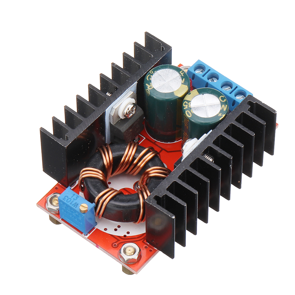
The module, presented in the photo below, measures 65 mm by 47 mm by 27 mm and weighs 60 grams. Two semiconductors are screwed onto heatsinks measuring 46 mm by 20 mm by 10 mm.
 |
| The QS-1224CBD module. (© 2022 Jos Verstraten) |
The specifications of the QS-1224CBD
- Input voltage: 10 Vdc ~ 32 Vdc
- Input current: 10 A max. without additional cooling
- Input current: 16 A max. with forced cooling
- Output voltage: adjustable, 12 Vdc ~ 35 Vdc
- Output current: 10 A max.
- Power: 100 W max. without additional cooling
- Power: 150 W max. with forced cooling
- Efficiency: 94 % typical
- Output ripple: 2 % max.
- Quiescent current: 25 mA typical
- Input stability: ±0.5 % typical
- Output stability: ±0.5% typical
- Temperature at maximum load: 45 °C typical
- Response time: 200 μs typical
Warning
The manufacturer warns on the site that the QS-1224CBD has no short circuit protection and no wrong polarity protection on the input.

The electronics of the QS-1224CBD
The circuitry of the QS-1224CBD is built around a UC3843A from Texas Instruments. This is a current controlled PWM controller. This chip works with a clock frequency of approximately 50 kHz that drives an N-MOSFET. The output pulse is PWM (Pulse Width Modulation), creating the control system responsible for setting the output voltage. On the two heatsinks are a HY1707 N-MOSFET with an RDS(ON) of only 6 mΩ and a Schottky diode MBR2045CT. That is a double diode of which only one is used. Two 1,000 μF capacitors are located between the two heatsinks, which sets alarm bells ringing in our minds about the maximum temperature to which those parts are exposed. On the other side of the PCB, shown in the photo below, we recognize a 78L10 voltage stabilizer, a UC3843A and a large SMD resistor of 0.01 Ω as the main components.
With help of the datasheet of the UC3843A and with the aid of a good magnifying glass, the schematic of this module can be accurately reconstructed. Our attempt is summarized in the diagram below, resistor and capacitor values are unfortunately not available.
The power supply for the UC3843A is provided by the 10 V stabilizer 78L10. The large capacitors between the heatsinks are of course the capacitors C1 and C6. They are located between the input voltage and ground and between the output voltage and ground. With the adjustment potentiometer R7, part of the output voltage is fed back to pin 2 of the UC3843A.
The operation of the circuit is as follows. As already written, the UC3843A supplies a PWM-pulse on pin 6. The on/off ratio of that pulse determines the value of the output voltage. When this pulse is 'H', the MOSFET T2 is turned on. A very large current will then flow from the VIN+ through the coil L1, the MOSFET T2 and the resistor R6 (0.01 Ω) to VIN-. However, the coil L1 resists the rise of that current by building up a large reverse voltage across itself. The left side becomes negative, the right side becomes positive. The diode D1 prevents the output voltage from being shorted to ground through the conductive MOSFET. If the pulse is 'L', the MOSFET is not conducting. The voltage across L1 is now in series with the input voltage between the ground and the anode of the diode D1. This diode starts to conduct and the output voltage becomes greater than the input voltage. This output voltage is smoothed again with capacitor C6.
Test conditions
Because the QS-1224CBD is advertised as a module that allows you to power all kinds of equipment from a 12 V battery, we took this situation as the starting point for our tests. The module is powered from a 12 V power supply that can deliver 30 A. This power supply is terminated with a capacitor bank of 10 x 1,000 μF. The input of the QS-1224CBD is connected to this bank. The inputs and outputs are terminated with capacitors of 100 nF on the PCB terminal block. The output is loaded with a constant current sink of type EBD-A20H.
It was decided to perform the tests with an output voltage of 24.0 V. This means that the module must double the input voltage and this should undoubtedly give a good impression of the capabilities of this circuit.
Output voltage range without load
At an input voltage of 12.05 V, we can set the output voltage between 11.85 V and 35.78 V with the adjustment potentiometer on the PCB. This is in accordance with the specifications, but we do have to make a critical remark. The output capacitor C6 has an operating voltage of only 35 V, so it is not very wise to set the output voltage higher than 30 V.
The output stability
The output stability specifies the constancy of the output voltage as a function of the output current. From the drop in output voltage, you can calculate the internal resistance of the converter using Ohm's law. Since the maximum power is specified as 100 W without additional cooling, the output current is limited to 5 A. The results are summarized in the table below. Over a load range of 0 A to 5.00 A, the output voltage drops by 127 mV. This corresponds to an internal resistance of 25.4 mΩ.
The noise and ripple on the output voltage
The output voltage is measured on the terminal block with the 1/10 probe of an oscilloscope. The image below shows the results with no load (left) and with a 100 W load (right). Note that the sensitivity is not set identically on both oscillograms: 200 mV/div with no load versus 500 mV/div with load. The results of this measurement are quite shocking:
- No-load: 507.0 mVpeak-to-peak and 47.49 mVrms
- Load: 1.537 Vpeak-to-peak and 199.5 mVrms
The long-term stability
In this test, the module output voltage is set to 24.0 V in a cold state and a 100 W (4.3 A) load is applied. The stability of the output voltage is measured as a function of time. The graph below shows that the module has a negative temperature coefficient. The output voltage drops by about 190 mV in thirty minutes and remains quite stable afterwards.
Thermal behavior
Although a high efficiency of 94% is specified, it is logical that, at maximum load, considerable heat is dissipated in the parts below:
- the schottky diode D1
- the MOSFET T2
- the electrolytic capacitor C6 over the output
- the coil L1
Those parts are close together on the PCB, so we are very curious how the module behaves thermally at the maximum load with 100 W at 24 V output voltage. We loaded the module for half an hour with a current of 4.3 A and then measured the temperature at the relevant points with a small thermocouple. The results are summarized in the illustration below.
Although modern electrolytic capacitors are allowed to have a working temperature of 105 °C according to various specifications, we do not feel completely happy when measuring such temperatures. All parts on the top of the PCB get very hot and it is logical that if you install the module somewhere in a case, the temperatures will rise even more.
The electronics of the QS-1224CBD
The circuitry of the QS-1224CBD is built around a UC3843A from Texas Instruments. This is a current controlled PWM controller. This chip works with a clock frequency of approximately 50 kHz that drives an N-MOSFET. The output pulse is PWM (Pulse Width Modulation), creating the control system responsible for setting the output voltage. On the two heatsinks are a HY1707 N-MOSFET with an RDS(ON) of only 6 mΩ and a Schottky diode MBR2045CT. That is a double diode of which only one is used. Two 1,000 μF capacitors are located between the two heatsinks, which sets alarm bells ringing in our minds about the maximum temperature to which those parts are exposed. On the other side of the PCB, shown in the photo below, we recognize a 78L10 voltage stabilizer, a UC3843A and a large SMD resistor of 0.01 Ω as the main components.
 |
| The components of the control system. (© 2022 Jos Verstraten) |
With help of the datasheet of the UC3843A and with the aid of a good magnifying glass, the schematic of this module can be accurately reconstructed. Our attempt is summarized in the diagram below, resistor and capacitor values are unfortunately not available.
The power supply for the UC3843A is provided by the 10 V stabilizer 78L10. The large capacitors between the heatsinks are of course the capacitors C1 and C6. They are located between the input voltage and ground and between the output voltage and ground. With the adjustment potentiometer R7, part of the output voltage is fed back to pin 2 of the UC3843A.
The operation of the circuit is as follows. As already written, the UC3843A supplies a PWM-pulse on pin 6. The on/off ratio of that pulse determines the value of the output voltage. When this pulse is 'H', the MOSFET T2 is turned on. A very large current will then flow from the VIN+ through the coil L1, the MOSFET T2 and the resistor R6 (0.01 Ω) to VIN-. However, the coil L1 resists the rise of that current by building up a large reverse voltage across itself. The left side becomes negative, the right side becomes positive. The diode D1 prevents the output voltage from being shorted to ground through the conductive MOSFET. If the pulse is 'L', the MOSFET is not conducting. The voltage across L1 is now in series with the input voltage between the ground and the anode of the diode D1. This diode starts to conduct and the output voltage becomes greater than the input voltage. This output voltage is smoothed again with capacitor C6.
 |
| The schematic of the QS-1224CBD. (© 2022 Jos Verstraten) |
Testing the QS-1224CBD
Test conditions
Because the QS-1224CBD is advertised as a module that allows you to power all kinds of equipment from a 12 V battery, we took this situation as the starting point for our tests. The module is powered from a 12 V power supply that can deliver 30 A. This power supply is terminated with a capacitor bank of 10 x 1,000 μF. The input of the QS-1224CBD is connected to this bank. The inputs and outputs are terminated with capacitors of 100 nF on the PCB terminal block. The output is loaded with a constant current sink of type EBD-A20H.
It was decided to perform the tests with an output voltage of 24.0 V. This means that the module must double the input voltage and this should undoubtedly give a good impression of the capabilities of this circuit.
Output voltage range without load
At an input voltage of 12.05 V, we can set the output voltage between 11.85 V and 35.78 V with the adjustment potentiometer on the PCB. This is in accordance with the specifications, but we do have to make a critical remark. The output capacitor C6 has an operating voltage of only 35 V, so it is not very wise to set the output voltage higher than 30 V.
The output stability
The output stability specifies the constancy of the output voltage as a function of the output current. From the drop in output voltage, you can calculate the internal resistance of the converter using Ohm's law. Since the maximum power is specified as 100 W without additional cooling, the output current is limited to 5 A. The results are summarized in the table below. Over a load range of 0 A to 5.00 A, the output voltage drops by 127 mV. This corresponds to an internal resistance of 25.4 mΩ.
 |
| The output stability of the QS-1224CBD. (© 2022 Jos Verstraten) |
The noise and ripple on the output voltage
The output voltage is measured on the terminal block with the 1/10 probe of an oscilloscope. The image below shows the results with no load (left) and with a 100 W load (right). Note that the sensitivity is not set identically on both oscillograms: 200 mV/div with no load versus 500 mV/div with load. The results of this measurement are quite shocking:
- No-load: 507.0 mVpeak-to-peak and 47.49 mVrms
- Load: 1.537 Vpeak-to-peak and 199.5 mVrms
 |
| Noise and ripple on the output voltage. (© 2022 Jos Verstraten) |
The long-term stability
In this test, the module output voltage is set to 24.0 V in a cold state and a 100 W (4.3 A) load is applied. The stability of the output voltage is measured as a function of time. The graph below shows that the module has a negative temperature coefficient. The output voltage drops by about 190 mV in thirty minutes and remains quite stable afterwards.
 |
| The long-term stability. (© 2022 Jos Verstraten) |
Thermal behavior
Although a high efficiency of 94% is specified, it is logical that, at maximum load, considerable heat is dissipated in the parts below:
- the schottky diode D1
- the MOSFET T2
- the electrolytic capacitor C6 over the output
- the coil L1
Those parts are close together on the PCB, so we are very curious how the module behaves thermally at the maximum load with 100 W at 24 V output voltage. We loaded the module for half an hour with a current of 4.3 A and then measured the temperature at the relevant points with a small thermocouple. The results are summarized in the illustration below.
Although modern electrolytic capacitors are allowed to have a working temperature of 105 °C according to various specifications, we do not feel completely happy when measuring such temperatures. All parts on the top of the PCB get very hot and it is logical that if you install the module somewhere in a case, the temperatures will rise even more.

This test clearly shows that the parts are too small and too close to each other. If capacitors with an operating voltage of 50 V were used, those parts would have a much larger cooling surface and would become less hot. The same, of course, applies to the two heatsinks. A larger PCB, so that the hot parts are further apart, would also help to lower the temperature of the whole.
 |
| The temperatures after half an hour of full power. (© 2022 Jos Verstraten) |
The input stability
The input stability indicates the constancy of the output voltage as a function of the input voltage. In view of the fact that this module has been developed for increasing a 12 V battery voltage, this is an important test. After all, the voltage across a lead-acid battery can vary from 10.8 V to 13.8 V. A good DC/DC-converter must keep its output voltage constant over this range.
Because our adjustable power supply is not capable of supplying sufficient current at a load of 100 W, we carried out this measurement with an output current of 2.0 A. The results are again summarised in the table below.
 |
| The input stability of the QS-1224CBD. (© 2022 Jos Verstraten) |
Our verdict on the QS-1224CBD
We would not dare to feed an expensive laptop from a lead-acid battery via this module. Although the measured temperatures do not exceed the specified limits of the parts, we still find that the total module gets too hot to be reliable. The test was performed at a room temperature of 23.5°C. Don't forget that the temperature in a car can reach up to 80°C in the summer! It will be clear that the parts will then become much hotter.
The very large high-frequency oscillations on the output voltage are also a reason not to use this module for powering sensitive and/or expensive circuits.
However, if you want to power a pair of 24 V LED strings from a 12 V lead-acid battery at a outdoor party, you can use this module without any problems.

QS-1224CBD DC-DC-convertor